External Lowpass Filter for UniTrunker design thread

Status
Not open for further replies.

SCPD

QRT
Joined
Feb 24, 2001
Messages
0
Location
Virginia
What is your timeframe with the circuit build and software changes?
Two or three weeks. This weekend is booked. The code is there.
Also, please PM me - I have code for LTR, Passport, and Multi-Net that works well. For Passport I have both normal and inverted versions. Ex. the NJ Transportation Authority (NJ Turnpike and Garden State Parkway Ops) uses inverted data.
My email is my username at radioreference.com.

Also let me know if you need me to beta test from here. There are many LTR, Passport, and one Multi-Net system in the area.
cool. Thanks!

Finally, not sure if you saw my question in the other thread, but what's your thoughts on a single radio option for Unitrunker?
it can be done. It's a low priority for me relative to everything else going on at the moment.
 
Last edited:

pro92b

Mutated Member
Premium Subscriber
Joined
Jun 27, 2002
Messages
1,910
A simulation for the 150Hz filter is in the attachment. The OPA340 is a single op amp but its model is the same for the OPA2340. C2, the input coupling capacitor, is shown as polarized but might be better as a nonpolar electrolytic like the Nichicon ES series. If polarized, the + terminal is oriented as shown for discriminator DC voltages greater than 2.5 volts (PRO-2006). Otherwise it should be reversed. R9 is recommended by the manufacturer to reduce overshoot caused by capacitive loads. Use the nearest 1% values for resistors and 5% capacitors. The circuit runs from a single 5 volt supply and needs just a few milliamps.

The attenuation at 300 Hz is about 18dB and becomes larger as the frequency is raised. To change to a 300Hz cutoff, cut the values of R5, R6, R7, and R8 in half. The circuit is taken from an EF Johnson design and a variant of this design is in use at my monitoring post.
 

Attachments

  • LTRfilter.jpg
    LTRfilter.jpg
    66.5 KB · Views: 316

jcardani

Member
Premium Subscriber
Joined
Jan 16, 2002
Messages
1,390
Location
Orlando, FL & Ocean City, NJ
Hi Pro92B

Very very nice! Great work!

BTW is there a substitute quad opamp available with similar characteristics as the OPA340? Just rather have one chip instead of 3 in the circuit.

thanks!
 

SCPD

QRT
Joined
Feb 24, 2001
Messages
0
Location
Virginia
I ordered about $30 in parts from Mouser this afternoon. I didn't find a source for OPA4340 or 2340 - at least not in a plastic DIP form.

Apparently the ICL7660 / MAX1044 is popular among do it yourself musicians for effect pedals. A cheaper LT1054 variant exists but they were out of stock.

I'd love to play with Bill's design as soon as I get a source.

For a separate project, I need a cheap crystal oscillator to use as a baud rate generator. Needs to be TTL compatible. Will clock a GAL16V8.
 

Mike_G_D

Member
Joined
Dec 19, 2002
Messages
1,241
Location
Vista, CA
This is an interesting thread; although I don't have a huge interest in decoding LTR stuff I do have some and agreeing on one good solid active filter design with a switchable or automatic bypass would be good move for the hobby!

I think Pro92b's design is bang-on. When I finally got around to reading this thread I, too, immediately thought why bother with a split Vcc supply? Just use ac coupling for the goesinna and goesoutta ports and divide the supply voltage in half for the bias for the op-amps and use rail-to-rail op-amps for best performance. Even with non-rail-to-rail op-amps I've done this many times back in the day with no problems. Now, the coupling/DC blocking caps might affect low frequency cutoff but I don't think that will be a problem in this case - a good non-polarized electrolytic like Pro92b chose should be fine. I see no reason that we need DC coupling for this circuit.

For the op-amp choice - just scan the data sheet for the OPA340, suggested by pro92b, and use it as a guideline in picking a more available close equivalent.

I wonder if maybe the bypass line tapped after the first stage (buffer amp) and used in 92b's design might inadvertently load down or otherwise affect the performance of some sound card inputs for the non-filtered input because of the active filter stage hanging off of it? At a minimum, I might use a 2K to 10K series resistor tapped off from between R4 and R5 of the 92b design and follow with a DC blocking cap - use another non-polarized electrolytic identical to the 10uF used for the input/output of the main circuit. Even better would be to tap off of the main input and add another dedicated buffer amp for the bypass line; that adds more complexity and cost but is the best way to go especially if you wind up using two dual op-amp IC's since you already have a spare op-amp available!

Also, just in case you aren't aware of it, keep in mind that 92b's schematic is from a simulation program - RLoad and Cload comprise the simulated load of the sound card input and are not part of the actual design of the external circuit. I am not sure about R9, though; it looks to be part of the design but I am not sure it's really needed though not a big deal if left in (it's only 10 ohms anyway in series).

-Mike
 
Last edited:

pro92b

Mutated Member
Premium Subscriber
Joined
Jun 27, 2002
Messages
1,910
My intention was to specify two dual op amps, type OPA2340. These are available from DigiKey in 8 pin DIP packages and take up just slightly more space than a quad op amp. The simulation schematic shows a OPA340 because that is the model TI provides for the OPA2340.

The two 8 pin DIPs contain a total of four op amps and the extra op amp can be used for a wideband buffer output if desired.

R9 is part of the design, recommended to stabilize the op amp under capacitive loading.
 

jcardani

Member
Premium Subscriber
Joined
Jan 16, 2002
Messages
1,390
Location
Orlando, FL & Ocean City, NJ
Here's Pro92B's schematic in ExpressPCB (ExpressSCH) format. Please let me know if any changes are needed. I also added a simple power supply circuit for those who needs it.

thanks,

Joe
 

Attachments

  • new bills.jpg
    new bills.jpg
    29.3 KB · Views: 343

Mike_G_D

Member
Joined
Dec 19, 2002
Messages
1,241
Location
Vista, CA
Umm, a few points here:

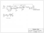
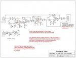
Again, as I wrote before, I strongly suggest that you put at least a cap and resistor inline on the bypass line. As you have it now, that line will have DC on it from the DC bias used on the op-amps. Also, where you have it tapped, between R4 and R5 it may be isolated enough from the inputs of the active filter stages from the point of view of the sound card input but you may still have issues wherein the sound card input may affect the filter operation - it depends on the input of the particular sound card used. I would play it safe and provide at least minimum isolation using a series 2K to 10K resistor and non-polarized electrolytic cap of the same value as C2 and C7 (10uF). Personally, I feel that it would be best to simply add another buffer stage in the bypass line - why take any chances? - if you end up using dual op-amp IC's then you have a fourth op-amp available anyway so why not use it?! Just add the same buffer amp design that is used in the main circuit (U1A) in the bypass line with ac coupling (DC blocking caps - same 10uF caps used on the main circuit). Just repeat the buffer stage including DC blocking caps both before and after it in the bypass line and you are good to go. Something I did forget to mention in my previous post though is that if you do this (use a separate buffer stage in the bypass line), then move the tap back to the point at the input (before C2) kind of like your first schematic; otherwise, if you don't use the fourth op-amp, then keep the tap where it is and at least add a series DC blocking cap of 10uF (non-polarized electrolytic, preferably) and a series resistor of 2K to 10K ohms (it can be higher and is not terribly critical but don't go lower than 2K, I think). But, as I said - if your using two dual op-amp IC's why not put the fourth op-amp to good use!

And since we're on the subject of dual op-amp IC's - in my experience, when creating a schematic depicting the use of multiple devices on multi-device IC's it is good practice to number the devices as UX-A, UX-B, etc. so as to show that you are using device 1 (say "U1-A") from the same IC as device 2 (say "U1-B"). In your schematic's case you have two U1's which would be better named as U1-A and U1-B (to indicate the two devices from the same IC). So, U2 would be U2-A and U2-B would be either unused or used as I suggested in the bypass line.

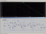
Finally, as I also stated in my previous post, those two components at the end of pro92b's schematic represent the simulated load of the sound card input used purely for his computer simulation as depicted in his post (that is why they are labeled "CLoad" and "RLoad" in his simulation schematic rather than using numbers like the other components). They are NOT part of the main circuit so should NOT be included in the schematic for the circuit as you have done; just delete C8 and R10.

I'd draw up a schematic for you but my only real schematic capture software from the old days is really old and I am not sure where the CD is hiding! If you have questions, though, feel free to PM me and we can sort it all out.

-Mike
 
Last edited:

pro92b

Mutated Member
Premium Subscriber
Joined
Jun 27, 2002
Messages
1,910
Here are my suggested changes.
 

Attachments

  • filter.JPG
    filter.JPG
    47.2 KB · Views: 293

jcardani

Member
Premium Subscriber
Joined
Jan 16, 2002
Messages
1,390
Location
Orlando, FL & Ocean City, NJ
Hi All,

My changes based on Mike GD and Pro92b's input. The last stage may still need some tweaking. Again, let me know if any changes are needed.

thanks,
 

Attachments

  • new bills.jpg
    new bills.jpg
    33.8 KB · Views: 302

pro92b

Mutated Member
Premium Subscriber
Joined
Jun 27, 2002
Messages
1,910
More updates
 

Attachments

  • filter.JPG
    filter.JPG
    58 KB · Views: 304

jcardani

Member
Premium Subscriber
Joined
Jan 16, 2002
Messages
1,390
Location
Orlando, FL & Ocean City, NJ
Changes made. I had to flip U2B in the schematic so the signal lines would not intersect and possibly confuse anyone. I also re-numbered some parts. It's late so please let me know if I got it right.

thanks,
 

Attachments

  • new bills 2.jpg
    new bills 2.jpg
    34 KB · Views: 249
Last edited:

Mike_G_D

Member
Joined
Dec 19, 2002
Messages
1,241
Location
Vista, CA
Yeah, that looks good to me; 92b must have suggested using the initial voltage divider to handle both the filter buffer and the bypass buffer - good idea, saves a few parts!

Sorry about snagging the extra op-amp UT!;-) Well, we could just say use two four op-amp IC's and label the extra IC something like "UT's Exclusive Reserved Op-Amp Cache - Reserved for UT's Exclusive Future Coming Attractions Use" or some such?!

BTW - UT, something to keep in mind - we are inverting the signal prior to spitting it into the sound card. I don't think that should be a problem for you but just highlighting it in case you might think of something funky resulting from that. A non-inverting solution could be designed if necessary, though, for me, I need to review my rusty op-amp design basics; 92b could probably whip it out in no time if desired, however.

-Mike
 

SCPD

QRT
Joined
Feb 24, 2001
Messages
0
Location
Virginia
I wanted the spare amp to serve as a second buffer amp. A switch would select between dual buffered audio or mono plus filtered audio.
 

pro92b

Mutated Member
Premium Subscriber
Joined
Jun 27, 2002
Messages
1,910
I have added capacitors to provide just a bit of filtering for the buffers. The buffer bandwidth is 50 kHz and that will serve to suppress the 450 kHz crud that comes out of the very commonly used MC1361 IF chip. The sound card doesn't have the bandwidth to respond directly to this high frequency but it is better to feed a clean signal to the PC and the small parts addition is worth it.

The switch allows two wideband channels or one wide plus one filtered.
 

Attachments

  • filter.JPG
    filter.JPG
    43.7 KB · Views: 258

SCPD

QRT
Joined
Feb 24, 2001
Messages
0
Location
Virginia
Replace the SPDT switch with a DPDT switch that also moves the input of U2B to a different mono input (for buffered audio from an indpendent source), that's where I was going.

This would allow accepting two independent control channel signals (unfiltered) or one signal in both buffered and filtered forms.
 
Status
Not open for further replies.
Top