I am making a usb radio transceiver which is based on PCB design. I made some troubles. Let me introduced the information I used here:
1.Hz Transceiver
2.MCP2210 USB-SPI Bridge
3.WM7087CT-ND
Even with just these three components and treview the PCB desgin knowledge which I get from Comprehensive Circuit Board Basics( Comprehensive Circuit Board Basics ), there are a huge number of things I'm uncertain about even after scouring the datasheets! I hesitate to ask them separately, since they are all closely related and it would be a waste of space to do so. Any and all help/answers is greatly appreciated.
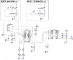
Here is my current working schematic: J3 is the USB port, U2 in the middle is the MCP2210, and U1 on the right is the RFM69HCW.
MCP2210 Questions:
1.Page 6 of the datasheet states that VUSB should be bypassed with a .22uF to .47uF capacitor. Will any value from that range work? What design considerations are there? (C8 in the schematic)
2.Page 6: What value bypass capacitors should I use for VDD? (C3 in the schematic)
3.Page 6: How do I know if I meet inrush requirements before building any of this?
4.Page 6: Do I really need to implement a Low-Power Suspend mode? Is it possible to just turn off the option so I don't need to worry about it? If I do need to implement it, what does that entail?
5.Page 8: What is the logical high voltage of the reset pin? 3.3V or 5V? I'm not sure which rail I need to connect the pullup to.
6.Page 9: Section 1.9 Oscillator, Note 1 states: "A series resistor may be required for quartz crystals with high drive level." This is the one I'm planning on using:*ECS-120-20-5PX-TR. Does it have a "high drive level"? If so, what resistance should I use?
RFM69HCW Questions:
1.I can't tell whether or not the SPI lines on the radio are OK with being 5V rather than 3.3V (since the MCP2210 datasheet states on page 6 that VDD sets the logic levels for SPI). How would I figure that out since I can't find it in the datasheet?
2.Is there anything special I need to do signal- or ground-plane-wise, since I have a radio/antenna on board? I've only done digital logic boards before.
3.Since the radio chip is the only slave, can I just tie its SS pin low so that it's always active? What pulldown value should I use? (R3 in the schematic)
4.The radio has three ground pins, but only one 3.3V input. Do I need decoupling caps between only the 3.3V and the closest ground pin, or between the 3.3V and*each*ground?
USB Questions:
1.What do I attach the USB case to?
2.Do I need to do any decoupling/bypass at the USB power pins?
All the information including the detail link and the schematic(attachment) have been given.
I am waiting for you help!
Thank you!


